In my last article I presented an overview of the LED cube, separating the design into three parts: the cube itself and the driver and controller circuits. This time I’m going to discuss the second one and emphasize the differences between the original building instructions and my solution.
Doing the math
Before we dive into the details of the driver circuit, we need to do some math regarding the timings and currents of our LED cube configuration.
I’m dreaming of playing fancy 3D animations on the cube once I’m finished. A visually smooth animation has 25-30 frames per second (FPS). To let each frame (a complete, yet still 3D image) stabilize before advancing to the next one, the whole cube should have a refresh rate around 100 Hz, which means this many frames will be displayed per second. Because in our case, the 3D image is created by quickly multiplexing eight 2D layers onto each other, the layer refresh rate is eight times higher than the frame refresh rate, resulting in 800 Hz. Calculating with the latter value further, we get 1 s / 800 Hz = 1.25 ms active time for a single layer. Assuming the 12.5% duty cycle we have calculated in the previous article, this means that each LED will be turned on and off for 1.25 ms and 8.75 ms, respectively. The original design had roughly 15 times faster refresh rates, but I find it to be an overkill, however if I experience some flickering I can easily boost the refresh rate from software.
The datasheet of the LEDs I have ordered from Ebay says that they can withstand a current of 30 mA for continuous operation or 70 mA peak current for momentary operation. Because the brightness of a LED is proportional to the current flowing through it, I’m planning to use the highest possible current. Although in theory the 1.25 ms active time and 12.5% duty cycle would qualify as momentary, I don’t want to overstress the LEDs during building and testing when they will be switched manually, so I decided to go with 30 mA.
The datasheet also states that the forward voltage of the LEDs are around 2.2 V. From this, we can calculate the size of the current limiting resistors required to achieve 30 mA through the LEDs.d Assuming 5 V supply voltage, the voltage on the resistor is 5 – 2.2 = 2.8 V and the required resistance is 2.8 V / 0.03 A = 93 Ω. However, after trying out one of the LEDs with a 100 Ω resistor, my measurements showed that the forward voltage is a little higher, so using a 82 Ω resistor would result in exactly 30 mA current flowing through the LED.
Driving columns
We need to control all 64 column terminals simultaneously. No microcontroller has this many I/O lines, so somehow we have to reduce the number of required outputs. I choose the shift register solution suggested in the original build instructions. This version uses 8-bit serial in parallel out shift registers. A shift register has 1 data input and 1 clock input terminal and 8 data output terminals. The data is shifted in serially one bit at a time in eight shift register clock cycles and then it can be read parallel on the eight data outputs. In this configuration the data outputs directly control 8 out of the 64 LED cube columns (I like to call this a row) via current-limiting resistors, so 8 shift registers cover all 64 columns organized in 8 rows.
The clock inputs of the shift registers are connected together, thus every shift register shifts their bits synchronously. Regarding the data inputs, we have two choices: we can either daisy chain the shift registers (the bit 7 of the previous shift register goes to the data input of the next one, so setting up a layer requires 64 shift register clock cycles), or we can fed the data to the shift registers parallel (each shift registers have an independent data input, thus only 8 shift register clock cycles is required to set up a layer’s state).
In the microcontroller, several instructions are required to manipulate the shift registers: fetching the next byte to show from the memory (2-3 instructions), shifting the bits (1-2 instruction), setting the data output pin (1-2 instructions), setting the clock output pin high and back to low (2 instructions), plus branching for loops (2-3 instructions). With the daisy chain configuration, this has to be repeated 64 times, resulting in 64 × 12 = 768 instructions. Assuming 1 MHz microcontroller clock frequency and RISC architecture (1 clock cycle per instruction), setting up a layer’s state requires 768 μs, so around 0.8 ms. Now recall the 1.25 ms layer active time we have calculated in the previous section. This means that in this configuration the microcontroller would spend most of it’s CPU time controlling the LEDs, leaving no time for anything else (computing animation frames or communicating with the computer).
Opposed to this, the parallel data feeding configuration (the one that is presented in the original build instruction as well) requires 8 times less instructions (0.1 ms estimated) at the cost of using 7 more I/O lines on the microcontroller. This seemed a reasonable compromise, so I ended up using the parallel data feeding configuration. The following schematic fragment shows the two different shift register chaining configuration (I show only 3 shift registers, but the principle remains the same).
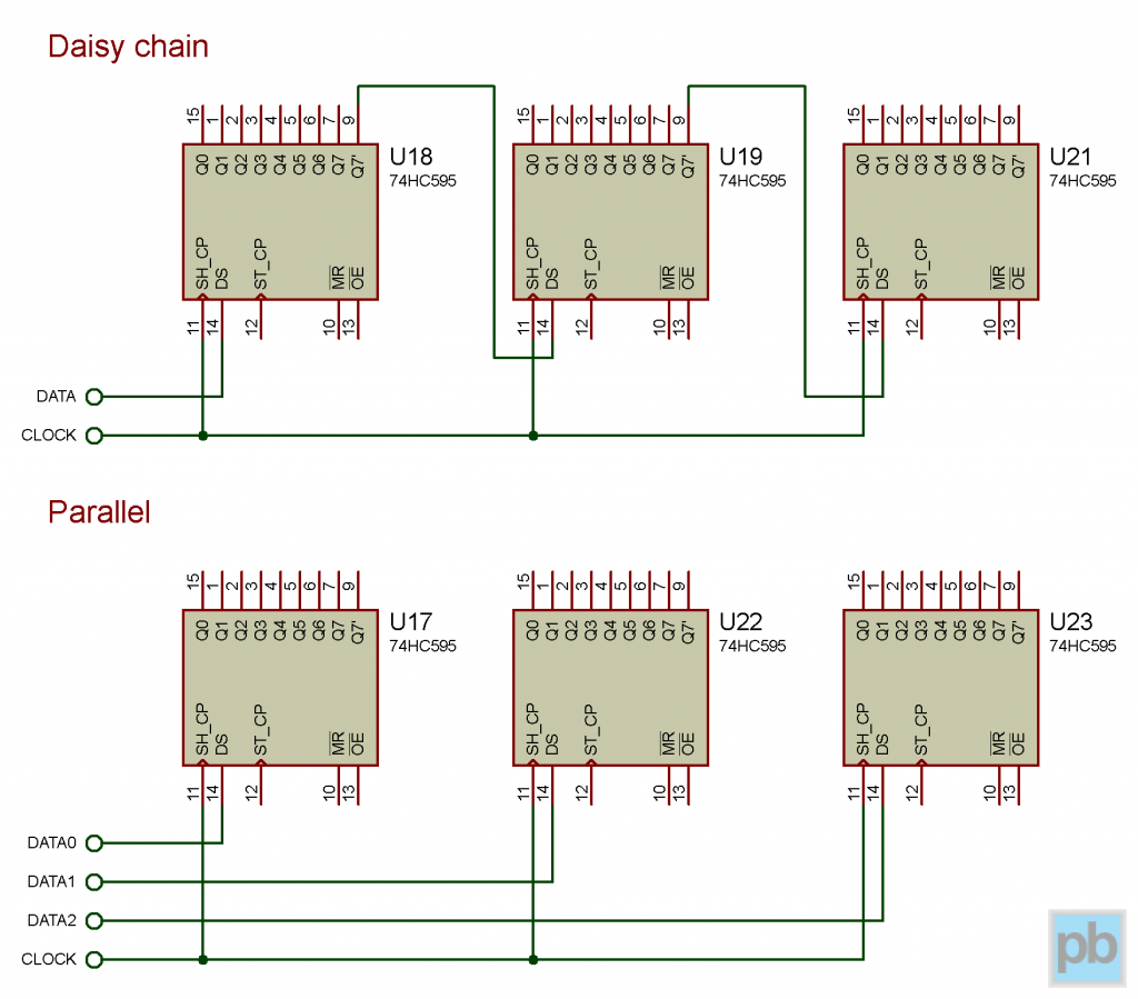 The original design suggests the 74HC164 shift register. However, the 74HC595 would be a better choice, because it has a built-in latch, so it retains its last output state until bit shifting the next state is finished, which results in reduced flickering of the outputs. This is a great explanatory video tutorial demonstrating the differences between the two components. Because of the latching functionality, the 74HC595 has an additional input pin for the latch control. With this in mind, my design requires 8+1+1 = 10 microcontroller I/O pins for controlling the columns.
So far so good, but if you read the 74HC595 datasheet carefully you can notice that although the shift register can handle 35 mA per output pin (showed as IOUT in the datasheet) – remember, I need 30 mA for my LEDs – that may be enough, but the whole IC cannot handle more than 70 mA (ICC) in total, so if more than 2 LEDs are active in a row at the same time, the shift register IC will most likely end in up smoke. This is unacceptable as there may be lot of 3D animations that require more than 2 LEDs per row.
To mitigate this problem one may use additional components to deal with larger currents like external transistors or the ULN2803 driver IC. While these are both valid solutions, I tried to minimalize the number of components (thus potential error sources both during calculations and assembly) in my design, so I choose the TPIC6C595 shift register instead. As its part number suggests, it has exactly the same functionality as the 74HC595, but it has open drain outputs which can handle up to 100 mA per pin even if all pins are turned on (ID in the datasheet).
If you aren’t familiar with the terms open drain or open collector (I weren’t also before starting this project), here is a great tutorial on how they work and how they can be used. There is a caveat you have to pay attention to when using open drain outputs. As this kind of output can only sink current (the current must flow into the pin towards the ground), all LEDs in the cube must have their negative (cathode) terminal connected to the shift register (they “point” towards the shift register on the schematic). This means the LEDs has to be wired in the direction “opposite” to the one presented in the original build instructions. As I wrote in my previous article all LEDs in a layer have their anode terminal connected and all LEDs in a column have their cathode terminal soldered together.
Driving layers
After figuring out how to control the 64 columns, let’s focus on controlling the 8 layers. Because the column driver logic uses 10 microcontroller I/O lines, I decided to save on layer controller lines by using a 3 to 8 line decoder IC which was not present in the original build instructions (or at least not for this purpose). A decoder has 3 inputs representing 3 address bits and 8 output lines of which one and only one is active at a given time selected by the address on the input – if the input is 000, 010 or 110 the output line 0, 2 or 6 is active, respectively. There are two decoder ICs in the 74x family: the 74HC138 and 74HC238 with the only difference that the first one has active-low while the second one has active-high outputs.
Since it is possible that all 64 LEDs are active at the same time in a given layer, we have to switch 64 × 30mA = 1.8 A, which is quite a lot. There isn’t any decoder ICs that can handle this much current, so we will need an external transistor. Since the LEDs that form a layer in the cube are connected together by their anode (positive) terminals (this is called the common-anode configuration) we have to switch the anodes (the positive power source terminal) to turn a layer on or off. This is called high-side switching (as opposed to low-side switching when we switch the ground terminal). The difference between the two is shown on the following schematic.
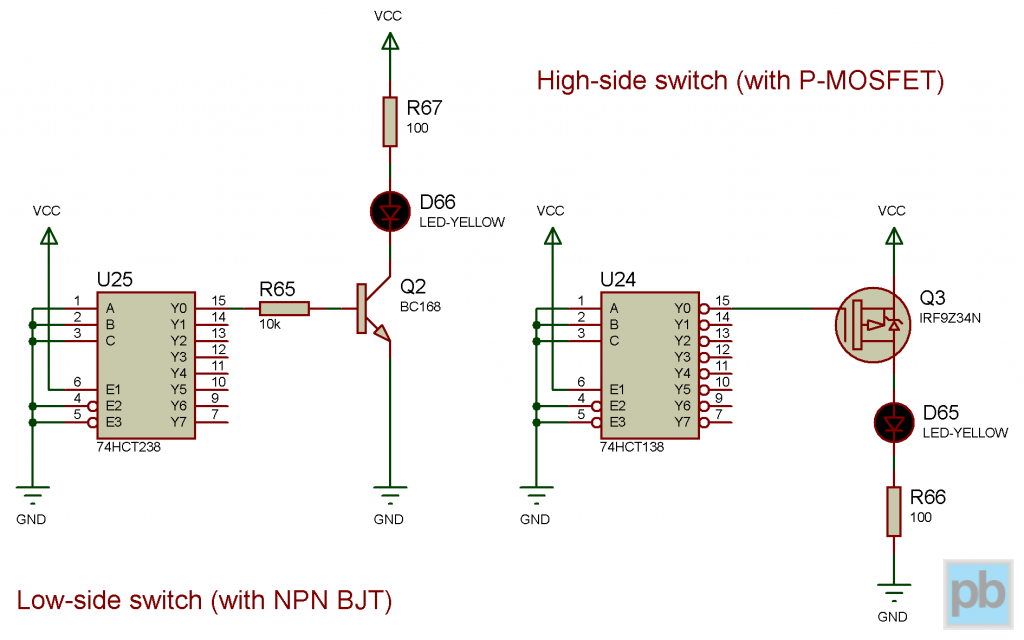
The next step is to decide whether to use traditional bipolar (BJT) or field-effect (MOSFET) transistors. BJTs are much cheaper so this was the first option I looked at. Bipolar transistors are current-controlled, the amount of current flowing through between the collector and the emitter is the function of the current flowing into or out from the base terminal. To switch 1.8 A on the high side with a PNP transistor, the base current exceeds 100 mA which is too much for the decoder IC. So we would need another transistor to control the first one, plus a few additional resistors (here and here are a few example circuits, though the latter uses the terms common anode and cathode incorrectly) that overly complicates the design.
In order to keep the circuit as simple as possible I choose MOSFETs over bipolar transistors despite their somewhat higher pricetag. For high-side switching only one P-channel MOSFET is required per layer without any additional components (the exact circuit is shown on the right side of the schematic above). Because MOSFETs are voltage-controlled there are no gate current limitations to deal with. However, we still need to carefully select an appropriate variant that is able to handle at least 2 A of source-drain current. I’ve chosen the IRF9Z34N that supports ID = 14 A maximum current as specified in the datasheet. The P-MOSFET is turned on (current flows between the source and drain terminals) if the gate terminal has negative (ground) voltage and turned off if the gate has high voltage attached to it. This implies that the MOSFET can easily be controlled with the active-low version (74HC138) of the decoder.
Getting it all together
Now that we have both parts – the column and layer driver – designed we can assemble the complete LED cube driver circuit that you can study on the following schematics.
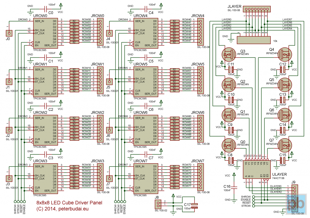
You can see the shift registers, current limiting resistors, the decoder and the layer controller MOSFETs and the connections to other main parts of the LED cube. JROW0-JROW7 and JLAYER are the connectors going to the LED cube column and layer terminals. J0-J9 are the connectors going to the controller circuit panel. J0 to J7 are the eight shift register data inputs, J8 is the 5 V power supply input and J9 is the connector for the IC control lines: shift register clock inputs and decoder address inputs. I’ve added two input lines I haven’t discussed so far. The first is the global reset line for clearing all shift register (and resetting the microcontroller itself on the controller panel), the second is an enable line that makes it possible to completely turn off the cube from the microcontroller by disabling the outputs of the shift register and the decoder.
There are also few additional components as well. There is a 10 kΩ pull-down resistor to aid properly turning off the layers. And there are some capacitors scattered around the schematic. These are required to deal with the sudden voltage drop running through the complete circuit when a layer with many active columns (thus large current need) is turned on. The capacitors are placed near every IC and MOSFET to sustain proper supply voltage to the digital circuitry even during a short temporary voltage drop.
Now that both the cube and the driver circuit is properly designed (I hope I haven’t made any miscalculations), I can finally start building the cube.
Hi, did you ever finished that cube and could share some code? Your design looks really great 🙂
Thanks for asking, the cube itself is finished, and it works perfectly. However, the microcontroller software needs more work, it was never finished. I had to put that project aside for a while now, but I will finish it some time 🙂
Nevertheless, I have the current state of the code on GitHub, so you can check it: https://github.com/peterbudai/cube